Leader in Advanced
Sample Preparation
Cybersecurity
-
Advanced IC deprocessing “tear down lab” enables high scalability to full IC X/Y dimensions while maintaining fine layer control in the Z-dimension. Utilizes a plug-and-play-style suite of mechanical, sputter, and chemical process methods across multiple instruments.
-
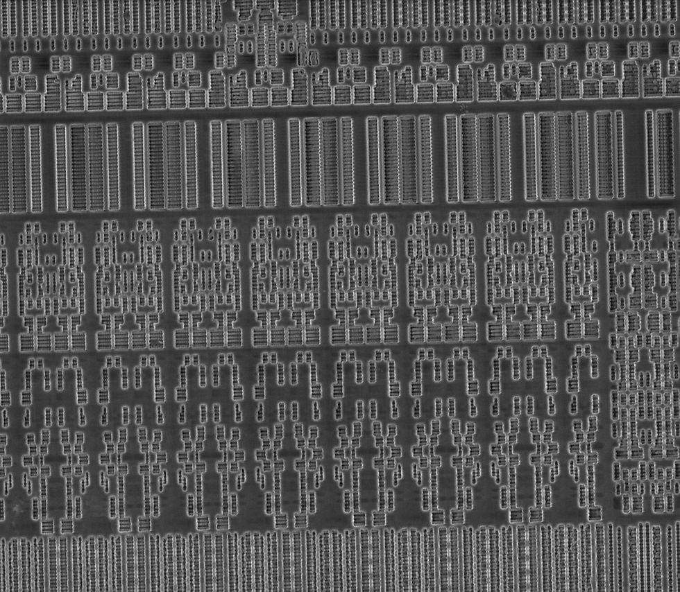
High throughput, high resolution imaging takes samples from the tear down lab images with nanometer scale resolution and full-dimension scalability using the Zeiss MultiSEM 505.
-
HPC computing processes multi-TB datasets to output structural image files. Image processing includes data navigation and alignment, sample and image setup feedback, and conversion to structural information files.


As new generations of IC’s and other microelectronics move to smaller and smaller node sizes, there is a need for novel QA/QC, V&V, and reverse engineering techniques that can resolve device structure at an incredibly small scale. Through our research and product development efforts, Varioscale aims to meet the needs of new device analysis with a novel suite of tools and methods that push the boundaries of imaging and sample deprocessing capabilities.